-
Whatsapp: +86 13526572721
-
Email: info@zydiamondtools.com
-
Address: AUX Industrial Park, Zhengzhou City, Henan Province, China
-
Whatsapp: +86 13526572721
-
Email: info@zydiamondtools.com
-
Address: AUX Industrial Park, Zhengzhou City, Henan Province, China
Diamond Wheels for Wafer Thinning: A Selection and Application Guide

What is the essential guide to selecting and using diamond wheels for wafer thinning?
This guide provides a complete overview for selecting and using diamond wheels in wafer thinning, covering the critical process stages from coarse grinding to final polishing. It offers specific wheel recommendations for different materials like silicon and SiC, and details an operator’s guide to optimal performance, including setting process parameters, wheel dressing, and troubleshooting common defects.
Understanding the Key Stages of the Wafer Thinning Process
So, how exactly does a thick, newly fabricated wafer become an ultra-thin slice ready for modern electronics?
The wafer thinning process is a multi-stage manufacturing sequence designed to precisely reduce a wafer’s thickness. It methodically moves from a rapid, high-volume material removal stage to a highly controlled, delicate finishing stage, ensuring the final wafer meets strict thickness, flatness, and surface quality specifications.
To achieve the incredible thinness required for today’s advanced chips, wafers can’t simply be ground down in one go. Instead, the process is carefully broken down into distinct stages. Each stage has a specific job, preparing the wafer perfectly for the next step. Think of it as a journey from brute force to a surgeon’s precision. Let’s walk through these critical stages one by one.
Stage 1: Coarse Grinding for Bulk Material Removal
The first step in the thinning journey is all about speed and efficiency. This stage is known as coarse grinding, or backgrinding.
The primary goal here is straightforward: to remove the majority of the unwanted material from the back of the wafer as quickly as possible. We aren’t concerned with creating a perfect, mirror-like finish yet. In fact, this process is quite aggressive. It is responsible for removing up to 90% of the total thickness that needs to be shed.
Imagine you have a thick plank of wood that you need to make much thinner. You wouldn’t start with fine sandpaper, would you? Of course not. You’d use a power planer to shave off thick layers quickly. Coarse grinding is the semiconductor industry’s equivalent of that power planer. It uses a diamond wheel with larger abrasive particles to achieve a very high material removal rate (MRR).
However, this speed comes at a cost. The aggressive nature of coarse grinding inevitably creates significant damage just below the wafer’s surface. This “sub-surface damage” consists of tiny micro-cracks and crystal lattice defects. From our experience in process engineering, a typical coarse grinding step might leave a damage layer that is 5-10 micrometers deep. This damage is an expected and accepted consequence of this stage because the next step is designed specifically to remove it.
Stage 2: Fine Grinding for Surface Integrity and Thickness Control
After the bulk of the material has been removed, the process shifts from speed to precision. Welcome to the fine grinding stage, where the focus is on quality, accuracy, and damage removal.
The main purpose of fine grinding is to carefully remove the sub-surface damage layer created during coarse grinding. At the same time, it brings the wafer to its final target thickness with incredible accuracy. This is where we start chasing perfection.
Continuing our analogy, this is like switching from the power planer to a high-quality orbital sander with fine-grit sandpaper. The material removal is much slower and more controlled. The goal now is to erase the rough marks from the previous step and produce a smooth, flat surface. In wafer thinning, fine grinding uses a diamond wheel with much smaller, finer abrasive particles.
This stage is absolutely critical for two key metrics:
- Total Thickness Variation (TTV): This measures how uniform the wafer’s thickness is from edge to edge. Poor TTV can cause problems in later packaging steps. Fine grinding aims to get TTV down to just a few microns, or even less. For example, on a 300mm wafer thinned to 75µm, a TTV target of under 3µm is common.
- Surface Finish: The process creates a smooth, semi-reflective surface by removing the micro-cracks. This prepares the wafer for the final finishing stage and ensures the final chip will be reliable.
By the end of this stage, the wafer is very close to its final form, but there is one final touch needed to ensure its structural integrity.
Stage 3: Final Polishing and Stress Relief
The final stage is all about stress management and achieving a flawless surface. Even after fine grinding, the wafer holds residual mechanical stress from the grinding process. If left unaddressed, this stress can cause the ultra-thin wafer to warp, bow, or even shatter during subsequent handling or dicing.
Therefore, the purpose of this final step is twofold: to relieve this internal stress and to create a perfect, mirror-like surface free of any remaining microscopic defects.
This stage often moves away from purely mechanical grinding and employs other techniques. One of the most common methods is Chemical Mechanical Polishing (CMP)1.
The Role of Chemical Mechanical Polishing (CMP)
CMP is a process that uses a chemical slurry and a polishing pad to gently remove the final few microns of material from the wafer’s surface. Unlike grinding, which is a purely mechanical action, CMP combines a chemical reaction (the slurry softens the surface) with mechanical abrasion (the pad wipes the softened material away). This hybrid approach is extremely gentle and effective at:
- Removing Residual Damage: It erases the last remnants of any sub-surface damage.
- Relieving Stress: The gentle, non-brittle nature of the removal process effectively relieves the mechanical stress built up in the wafer.
- Improving Surface Finish: It produces a superior, mirror-like surface with a roughness (Ra) of less than 1 nanometer.
After this final polishing and stress relief stage, the wafer is not only incredibly thin but also flat, stable, and structurally sound, making it ready for the demanding final steps of chip dicing and packaging.

Specific Wheel Recommendations for Your Grinding Application
Now that we understand the process, how do you choose the exact diamond wheel for your specific job?
Selecting the right diamond wheel requires matching its key properties—the bond, diamond grit size, and concentration—to the specific grinding stage and the wafer material. For standard silicon, a two-step approach with vitrified and resin bonds is typical. For hard materials like SiC, stronger bonds and different grit sizes are necessary to manage brittleness and achieve the desired finish.
Choosing a diamond wheel isn’t a one-size-fits-all decision. Using the wrong wheel is like trying to achieve a mirror finish on a lathe with a coarse roughing insert—the tool is simply not suited for the task and the result will be a failure. The material you are grinding is the single most important factor in your selection. We will break down our recommendations into the two most common scenarios faced in the industry: grinding standard silicon wafers and tackling much harder materials.
For Mainstream Silicon (Si) Wafer Thinning
Silicon is the workhorse of the semiconductor industry. Because it’s so common, the process for thinning it is well-established and highly optimized, typically using a two-stage grinding process with two very different types of wheels.
Wheel Recommendation for Coarse Grinding
For the initial, aggressive material removal stage, the clear industry choice is a vitrified bond diamond wheel2.
Think of a vitrified bond as a microscopic, ultra-hard ceramic sponge with diamond particles trapped inside. This rigid, porous structure makes it extremely tough and free-cutting. It holds its shape under high pressure and allows coolant to flow through its pores, which is essential for carrying away heat and ground material during high-speed grinding.
- Bond Type: Vitrified
- Grit Size: Typically in the range of #325 to #600. A coarser grit like #400 offers a great balance of high removal rate and manageable sub-surface damage.
- Concentration: A diamond concentration of 100 to 125 is standard, providing enough cutting points for efficient removal without excessive cost.
A Quick Note on Specifications: The exact grit size and concentration can vary slightly between wheel manufacturers. It’s always a best practice to consult your supplier’s datasheet to confirm the optimal specifications for your specific machine and process.
Wheel Recommendation for Fine Grinding
To remove the damage from the coarse grinding step and achieve a pristine finish, the process requires a shift to a much gentler wheel: the resin bond diamond wheel3.
A resin bond holds the diamond particles in a polymer matrix, almost like stones set in a hard epoxy. This bond is softer and has a slight dampening effect, which prevents it from being too aggressive. It acts as a shock absorber at a microscopic level, allowing the fine diamond particles to shear away material cleanly without creating new cracks. This is the key to achieving a smooth, damage-free surface.
- Bond Type: Resin
- Grit Size: Much finer, typically from #2000 to #4000. A #3000 grit wheel is a common choice for achieving a surface finish ready for the final polishing stage.
- Concentration: Generally lower, around 75 to 100, as the goal is surface refinement, not bulk removal.
For Hard-to-Grind Materials (SiC, GaN, Sapphire)
Materials like Silicon Carbide (SiC)4, Gallium Nitride (GaN), and Sapphire are rapidly gaining importance for high-power and optoelectronic applications. However, they are significantly harder and more brittle than silicon. Grinding them requires a different strategy and more robust tools.
Why can’t you just use the same wheels? Trying to grind SiC with a standard silicon wheel would be like trying to mill hardened tool steel with a high-speed steel (HSS) endmill instead of a carbide one. The tool would wear out instantly, and you would shatter the workpiece.
Wheel Recommendation for Coarse Grinding
For the coarse grinding of these hard materials, you need a bond with exceptional durability. The two primary choices are a metal bond wheel or a specialized, high-strength vitrified bond.
A metal bond wheel sinters the diamond particles into a metallic matrix, such as bronze. This creates an incredibly tough and wear-resistant cutting surface, capable of withstanding the immense forces needed to grind materials like sapphire.
- Bond Type: Metal or High-Strength Vitrified
- Grit Size: Often finer than what’s used for silicon, even for coarse grinding, typically in the #400 to #800 range. This helps to minimize the initial chipping and cracking on these brittle materials.
- Concentration: Higher concentrations of 125 to 150 are often necessary to provide enough cutting power and ensure a reasonable wheel lifespan.
Wheel Recommendation for Fine Grinding
For the finishing step, a specialized resin bond wheel is required. These are not the same as the resin wheels used for silicon; they are often formulated with unique fillers and resins to provide the right balance of cutting ability and fine finish on ultra-hard surfaces.
- Bond Type: Specialized Resin
- Grit Size: Extremely fine, ranging from #3000 all the way up to #8000, depending on the final surface finish requirement.
- Concentration: Similar to silicon fine grinding, a concentration of 75 to 100 is typical.
Quick Selection Reference Table
To make it even clearer, here is a simple table summarizing the starting recommendations for your wheel selection.
| Grinding Stage | Wafer Material | Recommended Bond Type | Typical Grit Size Range |
|---|---|---|---|
| Coarse Grinding | Standard Silicon (Si) | Vitrified | #325 – #600 |
| Fine Grinding | Standard Silicon (Si) | Resin | #2000 – #4000 |
| Coarse Grinding | Hard Materials (SiC, Sapphire) | Metal / Strong Vitrified | #400 – #800 |
| Fine Grinding | Hard Materials (SiC, Sapphire) | Specialized Resin | #3000 – #8000 |

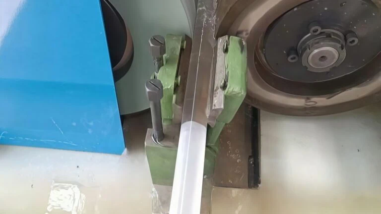
An Operator Guide to Optimal Grinding Performance
So, you have the right diamond wheel selected, but what specific operational settings and procedures are critical for high-yield wafer thinning?
High-yield wafer thinning relies on precise parameter control tailored to the specific material and grinding stage, including multi-step feed rates to manage stress. It also requires a proactive wheel conditioning strategy and a diagnostic approach to defects like TTV and sub-surface damage that are unique to thin wafers.
Having the correct wheel is the starting point, but repeatable, high-quality results come from mastering the machine. This is not about general grinding theory; this is about the specific recipes and techniques required to handle a fragile, high-value wafer. The following guide provides actionable starting points for the most common materials and procedures.
A Baseline Recipe for Mainstream Silicon Wafers
The following process recipes serve as a detailed, concrete starting point for the most common application in the industry: thinning standard 300mm silicon wafers. These parameters are optimized for balancing processing speed with high-quality results on silicon.
Coarse Grinding Recipe (Focus: Bulk Removal)
The goal here is to remove 80-90% of the target material quickly without introducing stress that could crack the wafer later.
| Parameter | Typical Setting | Operator’s Notes & Rationale |
|---|---|---|
| Spindle Speed | 1800 – 2200 m/min | This is the optimal speed range for most vitrified wheels to cut silicon efficiently. Running slower reduces removal rate; running faster can cause thermal stress. |
| Feed Rate Strategy | Multi-Step: 1. 3-5 µm/sec 2. 1-2 µm/sec | 1. Use the high feed rate for the bulk of removal. 2. In the final 50µm of this stage, step down the feed rate to reduce the depth of sub-surface damage. |
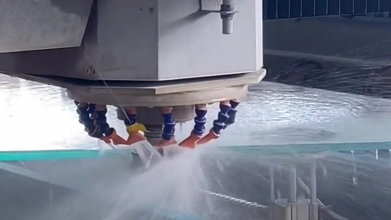
| Coolant Application | >10 L/min, dual nozzle | Use both in-spindle and external shower nozzles. You should see a consistent “bow wave” of DI water in front of the wheel, ensuring chips are flushed and the wafer stays cool. |
| Chuck Vacuum | > -85 kPa (or 25 inHg) | Verify a strong, stable vacuum before starting. Any fluctuation indicates a poor seal, which can cause wafer vibration and catastrophic failure. |
Fine Grinding Recipe (Focus: Damage Removal & Final Thickness)
This recipe is slower and far more delicate. The objective is to remove the damaged layer from the coarse grind and hit the final thickness target with minimal TTV.
| Parameter | Typical Setting | Operator’s Notes & Rationale |
|---|---|---|
| Spindle Speed | 1200 – 1500 m/min | The speed is deliberately lowered to reduce the mechanical impact on the wafer. This is crucial for producing a low-damage surface. |
| Feed Rate Strategy | Multi-Step: 1. ~0.5 µm/sec 2. “Spark-Out” | 1. Use this very slow feed to carefully remove at least 15µm of material, ensuring you get below the damage from the coarse step. 2. Add a “spark-out” pass: 1-2 table rotations with zero in-feed at the end to relieve stress and improve TTV. |
| Z-Axis Touch-Off | Use Non-Contact Sensor | Before grinding, the machine must precisely detect the wafer surface. A non-contact (optical or capacitance) sensor is essential to avoid chipping the wafer before the process even begins. |
| Total Material Removal | Minimum 15 µm | This is a critical rule. Removing less than this may not fully eliminate the deep cracks from the coarse grinding stage, leading to a weak die. |
Key Parameter Adjustments for Hard-to-Grind Materials (SiC, Sapphire)
When grinding hard, brittle materials like SiC or sapphire, the silicon recipe is no longer a direct guide but a conceptual baseline. The entire strategy must shift from a balance of speed and quality to a primary focus on “damage control.” Attempting to use silicon parameters on these materials will result in immediate and catastrophic wafer damage.
Here are the critical adjustments you must make:
Drastically Reducing Feed Rates
This is the single most important change. Due to their extreme brittleness, hard materials cannot withstand the mechanical shock of high-speed grinding.
- The Rule: As a starting point, reduce all feed rates by at least 50-70% compared to the silicon recipe.
- Practical Example: If the coarse grinding feed rate for silicon is 3 µm/sec, your starting feed rate for SiC should be no more than 1 µm/sec. For the fine grinding step, you may need to go as low as 0.1-0.2 µm/sec. The process will be significantly slower, and this is necessary and expected.
Optimizing Spindle Speed and Grinding Pressure
The goal here is to create a stable, low-vibration cutting environment.
- Spindle Speed: While the optimal speed depends on the specific wheel and material, it often involves a slight reduction from silicon parameters to minimize micro-vibrations that can propagate cracks in brittle materials.
- Grinding Pressure: The machine must apply force in a highly controlled manner. The strategy is “high rigidity, low pressure.” The machine must be stiff and stable, but the force exerted on the wafer should be minimized and applied gradually to avoid shock.
Adapting the Coolant and Dressing Strategy
Hard materials generate fine, abrasive swarf that can quickly clog a wheel.
- Coolant: High-flow coolant is even more critical here to aggressively flush chips away from the cutting zone and prevent the wheel from loading.
- Dressing: Since you are often using durable metal bond wheels (as discussed in Section 2), the dressing process must be more frequent and more aggressive to break down the tough bond and expose new diamond grits. This may require a different type of dressing stick and a dedicated dressing recipe.
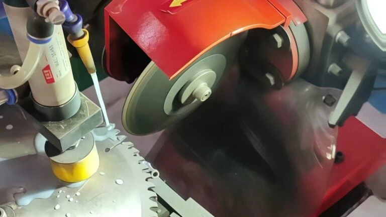
Proactive Wheel Conditioning: Beyond Basic Dressing
In wafer thinning, you cannot wait for a problem to appear before you maintain the wheel. A proactive conditioning strategy is essential for process stability.
Dressing Strategy: From Reactive to Predictive
While watching for signs of a dull wheel (like increased spindle load) is good, a world-class process doesn’t leave it to chance.
- Predictive Dressing: Establish a fixed dressing schedule based on your process data. A common strategy is to perform a wheel dressing5 cycle at the start of every new cassette of 25 wafers. This resets the wheel to a known, consistent state, preventing defects before they happen.
- Dressing Stick Selection: The stick must match the wheel. For a #400 grit vitrified coarse wheel, use a coarse, #100 grit white alumina (WA) dressing stick6. For a delicate #3000 grit resin fine wheel, use a much finer #600 grit WA stick to avoid damaging the wheel’s surface.
- Dressing Technique: Apply the stick with a slow, controlled feed rate (~10 µm/sec) across the entire wheel face. An incomplete or uneven dress will directly translate into poor TTV on your wafers.
A Diagnostic Guide to Wafer-Specific Defects
When thinning wafers to micron-level thicknesses, unique problems can arise. This guide focuses on wafer-specific defects and their root causes.
| Defect Observed | Common Wafer-Specific Causes | Recommended Actions for the Operator |
|---|---|---|
| Wafer Warpage / Bow (Wafer is shaped like a bowl) | 1. Grinding stress is too high. 2. No “spark-out” pass was used. | 1. Reduce the step-down feed rate in the coarse grind recipe. 2. Ensure a 1-2 rotation spark-out pass is included in the fine grind recipe. |
| Center Chipping / “Cratering” (Damage in the wafer center) | 1. Incorrect Z-axis “touch-off” procedure. 2. Excessive initial feed rate. | 1. Recalibrate the wheel’s non-contact height sensor. 2. Program a slower initial “ramp-down” feed for the first 5-10 µm of the cut. |
| High Sub-Surface Damage (SSD) (Hidden cracks below the surface) | 1. Fine grind did not remove enough material. 2. Fine grind feed rate was too aggressive. | 1. Verify the fine grind recipe removes at least 15µm more than the coarse grind damage depth. 2. Reduce the fine grind feed rate. |
| Backside Scratches (Post-Grind) (Marks appear after de-taping) | 1. Grinding swarf embedded in the protective backgrinding tape. 2. Rough handling during the de-taping process. | 1. Ensure the post-grind wafer clean/rinse cycle is working effectively. 2. Review wafer handling and de-taping procedures with the team. |
Conclusion
Successfully thinning wafers is a science that depends on a systematic approach. It begins with a solid understanding of the multi-stage semiconductor device fabrication process, transitions to selecting the precisely correct diamond wheel for the material, and culminates in the skillful application and maintenance of that wheel. By mastering these three pillars—the process, the tool, and the technique—operators can consistently overcome common challenges and produce high-quality, ultra-thin wafers that meet the demanding specifications of the modern semiconductor industry.
Ready to optimize your wafer thinning process? Contact our experts to get the ideal grinding wheels for your application.
References
- Chemical Mechanical Polishing (CMP)1 – The Wikipedia article providing a comprehensive overview of the CMP process, its history, and applications.
- vitrified bond diamond wheel2 – ZYDiamondTools product category for vitrified bond grinding wheels.
- resin bond diamond wheel3 – ZYDiamondTools product category for resin bond grinding wheels.
- Silicon Carbide (SiC)4 – The Wikipedia article for Silicon Carbide, detailing its properties, production, and applications.
- wheel dressing5 – ZYDiamondTools’ practical how-to guide for mastering the techniques of diamond wheel dressing.
- dressing stick6 – A product page for WA dressing sticks, a tool used for conditioning diamond grinding wheels.