-
Whatsapp: +86 13526572721
-
Email: info@zydiamondtools.com
-
Address: AUX Industrial Park, Zhengzhou City, Henan Province, China
-
Whatsapp: +86 13526572721
-
Email: info@zydiamondtools.com
-
Address: AUX Industrial Park, Zhengzhou City, Henan Province, China
How To Choose the Right Diamond Dicing Blade for Your Wafer Dicing Application
How do you select the exact diamond dicing blade configuration needed to maximize yield and prevent defects across various semiconductor materials?
To choose the optimal diamond dicing blade for your wafer dicing application, you must match the blade’s bond type, diamond grit size, and physical geometry directly to the hardness and brittleness of your specific substrate. Utilizing electroplated nickel bonds for standard bare silicon, durable metal sintered bonds for hard ceramics like SiC, and vibration-absorbing resin bonds for fragile compound semiconductors will effectively eliminate edge chipping, minimize kerf loss, and maximize total die yield.
Proven Blade Specifications for Bare Silicon Wafers
How exactly do you configure a dicing blade to slice through bare silicon without shattering the delicate die?
For bare silicon wafers, the industry standard is a hubbed electroplated nickel alloy blade. The integrated aluminum hub provides extreme rigidity, preventing blade wobble. Additionally, utilizing a fine diamond grit, typically in the 2 to 6-micron range, ensures clean cuts and virtually eliminates top and bottom edge chipping.
Why Hubbed Nickel Alloy Blades Excel in Standard Silicon Singulation
Silicon is a hard but extremely brittle material. Standard bare silicon wafers do not have the complex metallic layers found in advanced packaging. Therefore, they require a highly specific blade structure for clean singulation.
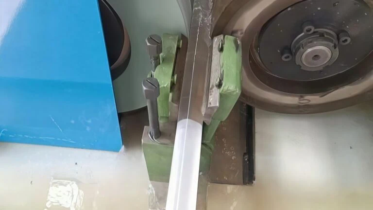
Hubbed blades feature a thin, diamond-impregnated cutting edge bonded directly to a thicker aluminum hub. Think of this aluminum hub like a rigid tool holder in a CNC milling machine. The tool holder grips the cutting bit closely to prevent it from bending under cutting pressure. Similarly, the aluminum hub supports the fragile cutting edge of the dicing blade. This strict support stops the blade from deflecting or wandering as it moves through the narrow silicon street.
Why do we specifically use an electroplated nickel alloy bond for these blades? Nickel electroplating tightly holds the diamond particles in place. This creates a very sharp and durable cutting edge. It also exposes a high percentage of the diamond points to the bare silicon. This high diamond exposure allows for a fast, cool cut.
Are hubless blades ever used for bare silicon? Yes, but they require separate metal flanges for mounting. This two-part setup can introduce microscopic vibrations. Vibration is the absolute enemy of a clean cut in brittle materials. Therefore, hubbed blades offer a superior, stable solution with guaranteed concentricity.
Typical cutting edge thicknesses for standard silicon range from 15 to 30 microns. However, maximum blade thickness limits can vary depending on your equipment. Always verify the exact thickness range compatible with your specific dicing saw spindle with your blade supplier.
| Blade Characteristic | Impact on Bare Silicon Singulation |
|---|---|
| Integrated Aluminum Hub | Maximizes rigidity, prevents blade deflection, and ensures straight cuts. |
| Electroplated Nickel Bond | Holds diamonds firmly and allows high diamond exposure for cooler cutting. |
| Pre-trued Edge | Eliminates the need for extensive blade dressing before production begins. |
Recommended Grit Sizes to Eliminate Top and Bottom Edge Chipping
Edge chipping is a major cause of expensive yield loss. Top chipping occurs on the top surface of the wafer. Bottom chipping happens where the blade exits the silicon and enters the dicing tape.
How do you stop this destructive chipping? The secret lies entirely in the diamond grit size.
Grit size refers to the physical size of the diamond particles embedded in the blade. Larger diamonds act like a coarse grinding wheel. They remove material quickly but leave a rough, fractured edge. Smaller diamonds act like fine lapping film. They remove material slowly but leave a very smooth, chip-free finish.
For bare silicon, minimizing mechanical stress is critical. Therefore, you must use a very fine grit size. The semiconductor industry standard uses diamond particles ranging from 2 to 6 microns. In traditional mesh sizes, this is roughly equivalent to #2000 to #4000 grit.
Why risk destroying an expensive silicon wafer just to cut slightly faster? A coarser grit will certainly increase your feed rate. However, the resulting severe bottom chipping will ruin the die. Finer grits do require a slightly slower feed rate. Yet, the profitable trade-off is a perfect, structurally sound edge.
Below is a breakdown of typical grit sizes for bare silicon processing.
| Grit Size (Microns) | Expected Cut Quality | Risk of Chipping | Typical Feed Rate |
|---|---|---|---|
| 2 – 4 μm (#4000) | Ultra-smooth finish | Very Low | Slow |
| 4 – 6 μm (#3000) | Excellent finish | Low | Moderate |
| 6 – 8 μm (#2000) | Acceptable finish | Moderate | Fast |
To completely eliminate bottom chipping, you must perfectly match this grit size to your spindle feed rate. A slower feed rate allows the fine diamonds to grind the silicon cleanly. If you push a fine-grit blade too fast, it will load up with silicon debris, overheat, and crack the wafer.

Tackling Hard and Brittle Substrates: Silicon Carbide (SiC) and Sapphire
How do you successfully dice incredibly hard materials like Silicon Carbide and Sapphire without rapidly destroying your blades or shattering the substrate?
To process hard and brittle substrates like Silicon Carbide (SiC) and Sapphire, you must use metal sintered bond diamond blades with tightly controlled diamond concentrations. The metallic matrix provides the extreme wear resistance required to withstand the high abrasion of these substrates. Furthermore, a precise balance of low feed rates and optimal diamond exposure prevents catastrophic material fracturing during the singulation process.
Metal Sintered Bonds for Maximum Wear Resistance in SiC Processing
Silicon Carbide (SiC)1 is exceptionally hard. It ranks around 9.5 on the Mohs hardness scale2. This extreme hardness quickly destroys standard blades. If you use a standard resin bond blade on SiC, the blade will lose its shape almost instantly. Therefore, you must select a metal sintered bond.
The Mechanics of Sintered Matrices
Metal sintered bonds mix diamond particles with metal powders, like bronze or iron. Manufacturers press and heat this mixture to create a solid metallic matrix. This matrix tightly grips the diamond grit.
Think of grinding a hardened tungsten carbide end mill. If you use a standard aluminum oxide grinding wheel, the wheel simply disintegrates. You must use a diamond grinding wheel with a tough bond. SiC behaves similarly during wafer dicing. It requires a robust metallic grip to hold the cutting diamonds in place.
The Self-Sharpening Advantage
The primary advantage of a metal sintered bond is its controlled wear rate. As the blade cuts the hard SiC wafer, the metal matrix slowly wears away. This gradual wear continuously exposes fresh, sharp diamond particles. Consequently, the blade maintains a consistent cutting ability throughout its lifespan.
Metal bond matrices vary significantly in their wear rates. A bond that is too hard will not expose new diamonds quickly enough. This causes the blade to glaze over and stop cutting. Therefore, selecting the correct bond hardness based on your specific SiC wafer thickness is critical.
| Bond Type | Wear Resistance | Suitability for SiC | Primary Drawback |
|---|---|---|---|
| Resin Bond | Low | Very Poor | Rapid blade depletion |
| Electroplated Nickel | Medium | Poor | Diamonds strip off quickly |
| Metal Sintered | Very High | Excellent | Requires precise feed rate control |
Balancing Diamond Concentration and Feed Rates for Sapphire
Sapphire is another incredibly demanding substrate. It has a Mohs hardness of 9.0. Furthermore, sapphire is highly prone to micro-cracking and severe edge chipping. To successfully dice sapphire, you must carefully balance the blade’s diamond concentration with your machine’s feed rate.
Understanding Diamond Concentration
Diamond concentration refers to the volume of diamond particles within the blade’s cutting edge. A high concentration means more diamonds are engaging the sapphire simultaneously. This distributes the cutting force across more points.
However, high concentration blades leave less room for the bond material. They also leave less space for coolant to flush away the microscopic sapphire dust. If dust builds up, friction increases rapidly. This friction generates immense heat, which will crack the fragile sapphire die.
Optimizing the Feed Rate
Because of this friction risk, you cannot cut sapphire quickly. You must use extremely slow feed rates. Typical feed rates for sapphire range from 0.5 mm/s to 2.0 mm/s.
Imagine pushing a fine-tooth metal cutting band saw through a thick block of hardened tool steel. If you push the material too fast, the teeth will load up, overheat, and snap. You must let the teeth do the cutting at a slow, steady pace. Dicing sapphire follows the exact same principle.
Optimal feed rates depend heavily on your exact spindle power and blade thickness. Consequently, you should confirm the recommended starting feed rate parameters with your blade manufacturer.
| Diamond Concentration | Blade Life | Feed Rate Requirement | Risk of Overheating |
|---|---|---|---|
| Low (e.g., 50) | Shorter | Can be slightly faster | Lower |
| Medium (e.g., 75) | Average | Moderate (1.0 mm/s) | Moderate |
| High (e.g., 100) | Longer | Must be very slow (<1.0 mm/s) | High |
By selecting a medium-to-high diamond concentration and pairing it with a strictly controlled, slow feed rate, you can minimize stress. This specific combination is the key to achieving clean, chip-free edges on sapphire wafers.

Handling Compound Semiconductors: Gallium Arsenide (GaAs) and Indium Phosphide (InP)
How can you successfully dice incredibly fragile compound semiconductors like Gallium Arsenide3 or Indium Phosphide without shattering the expensive wafers into dust?
To process highly brittle compound semiconductors, you must use ultra-thin resin bond diamond blades. The resin matrix acts as a microscopic shock absorber, providing a stress-free cut that prevents the propagation of micro-cracks. Furthermore, employing the thinnest possible blade geometry significantly reduces kerf loss, preserving valuable substrate material and maximizing your total die yield per wafer.
Using Resin Bond Blades for Stress-Free Cutting of Extremely Fragile Substrates
Compound semiconductors like GaAs and InP have very distinct, fragile cleavage planes. This means they fracture extremely easily under any mechanical pressure. If you use a rigid metal bond blade, the sheer force of the cut will instantly propagate micro-cracks across the wafer. Therefore, a resin bond is the absolute requirement for these materials.
What exactly is a resin bond4? It is a composite that combines diamond abrasive with a phenolic or polyimide matrix. This plastic-like matrix is inherently softer and more compliant than metal. During the high-speed dicing process, the resin actually absorbs microscopic vibrations.
Think of it like using a compliant lapping pad on delicate precision optics, rather than grinding them with a rigid stone wheel. The soft backing prevents destructive impact damage. The blade gently grinds away the material without imparting excessive mechanical stress into the die.
Because the resin wears away easily, it constantly exposes fresh, sharp diamond edges. This continuous self-sharpening action ensures a very low-friction cut. However, this fast wear rate naturally results in a shorter overall blade life. You must weigh the cost of replacing the blade against the high value of a perfectly cut GaAs wafer.
| Bond Type | Vibration Absorption | Risk of Cleavage Fractures | Suitability for GaAs/InP |
|---|---|---|---|
| Metal Sintered | None | Extremely High | Never recommended |
| Electroplated Nickel | Low | High | Poor |
| Resin Bond | High | Very Low | Industry Standard |
Minimizing Kerf Loss with Ultra-Thin Blade Geometries
Compound semiconductor substrates are exceptionally expensive to manufacture. Every single micron of wasted material directly impacts your bottom line. Therefore, minimizing “kerf loss5“—the total width of the material removed by the blade—is a critical engineering priority. You achieve this tight tolerance by selecting ultra-thin blade geometries.
For GaAs and InP production, process engineers frequently specify blades with cutting-edge thicknesses between 10 to 15 microns. By drastically reducing the blade thickness, you can design much tighter scribe lines (streets) on the wafer map. This dense layout allows you to fit significantly more functional die onto a single substrate.
In a precision CNC machine shop, if a machinist needs to part off a highly expensive block of aerospace titanium, they will use the absolute thinnest slitting saw available to save raw material. Wafer dicing operates on the exact same economic principle. You want to separate the components cleanly, not grind precious material into expensive dust.
However, utilizing ultra-thin blades introduces a new challenge. They lack lateral rigidity and are highly susceptible to deflection, or wandering, during the cut. To counteract this physical limitation, these blades require specialized mounting.
| Blade Thickness | Expected Kerf Width | Deflection Risk | Recommended Mounting Strategy |
|---|---|---|---|
| 10 μm | ~12 μm | Very High | Maximum diameter precision flange |
| 15 μm | ~17 μm | Moderate | Standard precision flange |
| 20 μm | ~22 μm | Low | Standard flange |
To maintain a perfectly straight cut, you must support the thin blade with high-precision flanges. These flanges grip the blade tightly, extending as close to the cutting edge as physically possible. This maximizes rigidity and ensures the blade stays perfectly on the programmed path.

Blade Selection for Advanced Packaging and Embedded Wafers (QFN, BGA, EMC)
Successfully separating complex advanced packages requires overcoming severe material density differences that can easily gum up standard tools.
To successfully dice advanced packages like QFNs and BGAs, you must select specially formulated blades that manage the drastic density differences between soft plastics and hard metals. Specifically, using blades with lower diamond concentration prevents epoxy loading, while precisely calculating blade exposure ensures you can slice through thick copper leadframes without causing blade deflection or metallic burrs.
Overcoming Blade Loading When Dicing Epoxy Molding Compounds
Epoxy molding compound (EMC)6 is a standard encapsulant in advanced packaging. However, cutting EMC presents a unique mechanical challenge. Unlike brittle silicon, EMC is soft and highly susceptible to thermal melting.
During the dicing process, friction generates heat. This heat slightly melts the EMC. The sticky, melted plastic then flows into the microscopic spaces between the diamonds on your blade. Engineers refer to this destructive process as “blade loading.”
Think of grinding a block of soft aluminum with a very fine-grit surface grinder. The soft aluminum quickly melts and completely clogs the grinding wheel’s abrasive pores. The wheel stops cutting and simply rubs against the metal, creating even more heat. Blade loading in EMC works on the exact same principle.
When a dicing blade loads up, it stops cutting efficiently. Friction spikes aggressively. This extreme heat can warp the package, melt the die attach film, or ultimately snap the blade. To prevent this, you must prioritize “swarf clearance.” Swarf is the waste material created during the cut.
You achieve better swarf clearance by selecting a blade with a lower diamond concentration. A lower concentration means there is more physical space between the individual diamond particles. This extra space acts as a channel, allowing the coolant to flush the sticky EMC swarf away before it can harden.
| Diamond Concentration | Swarf Clearance Capacity | Risk of Blade Loading | Suitability for EMC |
|---|---|---|---|
| High | Very Poor | Extremely High | Not Recommended |
| Medium | Moderate | Moderate | Acceptable for thin layers |
| Low | Excellent | Very Low | Highly Recommended |
Additionally, utilizing specialized resin bond formulas can help. Some resin bonds are designed to wear away quickly, constantly exposing fresh, unclogged diamonds. Because resin bond compositions for EMC vary significantly across the industry, carefully evaluating the exact bond hardness and porosity specifications is necessary.
Optimizing Blade Exposure for Thick Copper Leadframes
Quad Flat No-lead (QFN) packages often feature thick copper leadframes. Copper is incredibly ductile and gummy. It does not fracture cleanly like silicon. Instead, the blade must tear through the metal. This tearing action places enormous lateral stress on the thin dicing blade.
To handle this stress, you must optimize your “blade exposure.” Exposure is the exact length of the cutting edge that extends beyond the rigid metal mounting flange.
If your exposure is too long, the blade acts like a diving board. It becomes flimsy. When it hits the tough copper layer, the blade will bend or deflect. This deflection causes curved cuts, wide kerfs, and unacceptable copper burrs along the package edge.
Consider a machinist using a parting tool on a metal lathe. If the machinist extends the thin parting tool too far from the rigid tool post, the tool will chatter, vibrate violently, and eventually break. Wafer dicing requires the exact same rigid setup.
Conversely, if your exposure is too short, the metal flange will physically crash into the top of the EMC package. This will instantly destroy the device.
Therefore, you must calculate the minimum possible exposure. A standard industry practice is to take your maximum required cutting depth and add a strict safety margin of 0.2mm to 0.3mm. This calculation provides enough clearance to cut through the package and into the dicing tape, while maximizing the blade’s structural rigidity.
Selecting Multi-Step Cutting Strategies for Heterogeneous Materials
Advanced packaging7 contains a mix of radically different materials. A single BGA might contain a brittle silicon die, a sticky EMC overmold, and a ductile copper substrate. Unfortunately, a blade optimized for brittle silicon will struggle immensely with ductile copper.
How do you solve this material conflict? You utilize a multi-step cutting strategy, commonly called “Step Cut” or “Dual Cut.”
This process uses a dual-spindle dicing saw. The machine performs the separation in two distinct passes, utilizing two entirely different blades.
Think of a CNC routing operation on a composite panel. A machinist will first use a heavy-duty roughing endmill to remove the tough outer layers quickly. Then, they will switch to a high-precision finishing endmill to create the final, clean dimensions. Step cutting applies this logical workflow to micro-electronics.
In a typical step cut for a QFN package:
- Step 1 (Partial Cut): The first spindle uses a thicker, lower-concentration blade. This blade is engineered specifically to cut through the sticky EMC and the brittle silicon die without loading. It stops just above the copper layer.
- Step 2 (Full Cut): The second spindle follows directly behind the first. It uses a thinner, specialized electroplated or resin blade designed explicitly for ductile metals. This blade cuts through the remaining copper leadframe and slightly into the dicing tape.
| Process Stage | Target Material | Ideal Blade Characteristics | Primary Goal |
|---|---|---|---|
| Step 1 Cut | EMC & Silicon | Thicker, low concentration | Prevent loading and silicon chipping |
| Step 2 Cut | Copper Leadframe | Thinner, high wear resistance | Prevent copper burring and blade deflection |
By dividing the labor, each blade only cuts the material it was designed to handle. Consequently, you dramatically reduce copper smearing, eliminate silicon chipping, and significantly extend the lifespan of both cutting tools.

Actionable Troubleshooting Adjustments for Immediate Yield Improvement
When sudden edge chipping or blade wandering occurs, replacing your entire dicing setup is rarely the first logical step.
To immediately improve wafer yield, you must synchronize your spindle RPM with the blade’s diamond concentration to maintain the correct cutting speed. Simultaneously, you must adjust your coolant nozzles to precisely target the blade’s leading edge, ensuring maximum heat reduction and efficient swarf removal.
Synchronizing Spindle RPM with Diamond Concentration to Prevent Deflection
Spindle speed directly controls how the diamond particles interact with the substrate. You measure this speed in Revolutions Per Minute (RPM)8. Consequently, you must match your RPM to your blade’s diamond concentration. If you fail to do this, the blade will deflect. Deflection causes curved cuts and ruins your delicate wafer streets.
Think of a standard CNC milling machine. A machinist uses a four-flute endmill differently than a two-flute endmill. The four-flute tool has much less space between the cutting edges. Therefore, it requires specific spindle speeds to clear metal chips properly without snapping. Dicing blades work the exact same way.
High-concentration blades pack many diamonds tightly together. As a result, they have very little space to clear debris. If you run a high-concentration blade at an extremely high RPM, the blade will glaze over. The diamonds quickly become dull. The blade stops cutting and simply rubs against the wafer, creating immense heat. This lateral friction physically pushes the thin blade off its straight path.
To fix this glazing issue, you must lower the spindle RPM. A lower RPM allows the blade’s bond to wear properly. This gradual wear continuously exposes fresh, sharp diamonds.
Conversely, low-concentration blades need a higher RPM. They have fewer diamonds doing the actual cutting work. Therefore, they must spin faster to maintain a smooth, continuous cutting action.
“Matching your spindle RPM to your specific diamond concentration is the fastest way to correct blade wandering during active production.”
Because optimal RPM ranges vary significantly based on your specific saw manufacturer and the blade’s outer diameter, always verify the exact speed limits with your equipment supplier before making drastic changes.
Precision Coolant Flow and Nozzle Positioning for Effective Swarf Removal
Coolant does much more than just lower the cutting temperature. It actively flushes microscopic waste, called swarf, out of the cutting channel. If swarf builds up in the kerf, friction spikes immediately. This sudden friction destroys the wafer edge. Therefore, precise coolant application is absolutely mandatory.
Imagine deep-hole drilling on an industrial lathe. If the machinist does not use high-pressure, through-tool coolant to push the metal chips out of the hole, the drill bit will bind and snap instantly. In wafer dicing, the narrow street acts exactly like that deep hole. You must constantly flush it out.
Your nozzle positioning is highly critical. You cannot simply spray water randomly at the spinning blade. Instead, you must aim the primary cooling nozzle exactly at the leading edge. This is the exact micro-point where the blade first enters the substrate material.
Furthermore, you must strictly control the coolant flow rate. A flow rate that is too low will cause the blade to overheat, warp, and crack the die. However, a flow rate that is too high causes a dangerous physical problem called hydroplaning.
During hydroplaning, the thin blade actually rides on a high-pressure wedge of water. This intense pressure pushes the blade sideways, causing severe deflection and uneven cut depths.
| Defect Symptom | Likely Coolant Cause | Required Nozzle Adjustment |
|---|---|---|
| Severe blade overheating | Flow rate is too low | Increase flow, check system pump pressure |
| Blade wandering (hydroplaning) | Flow rate is too high | Decrease flow, adjust nozzle angle downward |
| Heavy swarf buildup in kerf | Incorrect target point | Aim precisely at the blade’s leading edge |
Always ensure your coolant water is highly purified and properly filtered. Contaminants in the water will act as unwanted abrasives, which will prematurely destroy your diamond blade’s cutting edge.
Conclusion
Maximizing yield in the wafer dicing process is never a matter of guesswork; it requires precise engineering and a thorough understanding of material science. By carefully evaluating the hardness, brittleness, and composition of your substrate, you can accurately specify the necessary bond type, diamond grit size, and blade geometry. Whether you are dealing with brittle bare silicon, extremely hard sapphire, or heterogeneous advanced packaging, the right blade configuration exists to optimize your process.
For application-specific blade recommendations or custom troubleshooting support, please contact us for further assistance.
References
- Silicon Carbide (SiC)1 – ScienceDirect topic page covering the material properties and applications of Silicon Carbide.
- Mohs Hardness Scale2 – Geology.com explanation of the Mohs hardness scale for identifying minerals.
- Gallium Arsenide3 – Wikipedia article explaining the properties and applications of the compound semiconductor Gallium Arsenide.
- Resin Bond Wheels4 – ZYDiamondTools guide detailing the selection and application of resin bond diamond wheels.
- Kerf5 – Wikipedia section explaining the concept of kerf and material loss during cutting processes.
- Epoxy Molding Compound (EMC)6 – Wikipedia page detailing the composition and use of EMCs in semiconductor packaging.
- Advanced Packaging7 – Wikipedia article on the definition and methods of advanced semiconductor packaging.
- Revolutions Per Minute (RPM)8 – Wikipedia article defining RPM as a measure of rotational speed.